Spot Melting
Problem ‐ Challenges with Line Melting
Electron beam powder bed fusion (E-PBF) is highly suited for producing complex, high‐performance parts with superior material properties. The conventional technique of line melting involves using an electron beam to melt a path along a straight or curved line. While this approach is simple and reliable, it poses several challenges:
- Thermal Restrictions: Material properties are highly influenced by the thermal history experienced during manufacturing. In line melting, the electron beam must linger along a path to melt it completely, leading to an accumulation of heat. This lack of optimal control over melting can result in variations in material properties.
- Limited Microstructural Control: Fine‐tuning microstructures within a part is critical for tailoring its mechanical and functional properties. However, the confined nature of line melting makes it challenging to achieve precise control over microstructures, limiting the ability to optimize material performance.
- Lateral Material Displacement: The process of line melting can displace material laterally over the melt surface, causing unintended distortions or variations in the part’s geometry.
- Hard to automate: When aiming for automated build file creation, it is hard to effectively fit straight lines onto a complex build area. This difficulty increases when trying to apply curved lines. This impedes the development of software geared towards automating the creation of build files.
Solution ‐ Spot Melting
To address these challenges and provide researchers with enhanced control over the manufacturing process, spot melting is a solution. Advantages of spot melting include:
- Enhanced Thermal Profile Control: Spot melting empowers researchers to precisely control the thermal profile within the build area. By melting material in discrete spots, heat accumulation is minimized, resulting in improved material properties and consistency.
- Microstructural Control: The ability to create melt pools rather than lines facilitates the creation of intricate microstructures. Researchers can fine‐tune the arrangement and composition of these spots, leading to enhanced mechanical properties and tailored performance.
- Elimination of Lateral Displacement: Spot melting eliminates the issue of lateral material displacement, ensuring that the desired part geometry is faithfully reproduced without unintended distortions.
- Less geometry dependent: Spot melting offers greater ease in creating both straight and curved features, simplifying the manufacturing of parts with complex geometries.
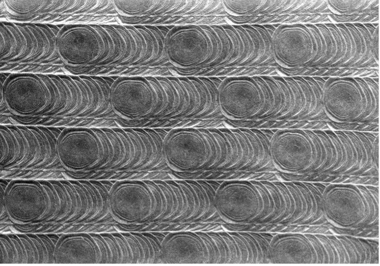
 Figure 1: Spot melting pattern on the top surface of a build, built in a Freemelt ONE.
Spot Melting with Freemelt ONE
Freemelt ONE is a research‐focused E-PBF platform optimized for spot melting. It has several features that makes Freemelt ONE a suitable platform for utilizing spot melting for research:
- High Beam Power: With a high power output of up to 6 kW, the Freemelt ONE opens up a broad spectrum of material possibilities, enabling researchers to explore a wide range of alloys and composites while conducting experiments. Additionally, a high powered beam allows for rapid melting, enabling more spots to be melted in a given timespan.
- Rapid Traverse Speed: The Freemelt ONE achieves traverse speeds of up to 4000 m/s, enabling efficient spot melting even across expansive build areas. This exceptional speed, along with the high beam power, allows the electron beam to melt tens of thousands of positions within a single second.
- Pixelmelt® Cloud Software: The cloud‐based Pixelmelt® software further elevates the spot melting capabilities of the Freemelt ONE. By automatically dividing the build area into individual pixels and applying a variety of algorithms for melting, researchers can efficiently conserve precious time when generating build files. Pixelmelt® is highly configurable, preserving Freemelt’s core philosophy of providing users with substantial control over the manufacturing process.
![]() Figure 2: Pixelmelt® patterns scanned and recorded in a Freemelt ONE.
Figure 2: Pixelmelt® patterns scanned and recorded in a Freemelt ONE.
Conclusion
Spot melting grants new capabilities, including refined thermal and microstructural control, as well as a greater potential for automating build file creation. Freemelt ONE excels at spot melting by harnessing its high beam power, rapid traverse speed, and Pixelmelt® cloud software, making it a uniquely fitting platform for enhanced control and innovation within E-PBF.
Learn more about Freemelt ONE.
Learn more about Pixelmelt®.
2023-09-19 10:11:45
