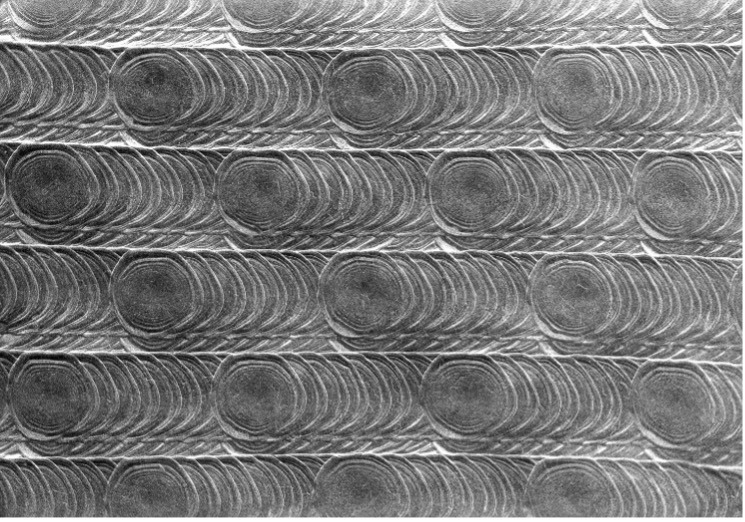
E-PBF + SEM = True!
If you have a scientific interest, you may have reflected upon the similarity between a scanning electron microscope (SEM) and an electron beam powder bed fusion (E-PBF) machine.
An SEM is composed of an electron gun and a high vacuum chamber. The electron gun scans an e-beam over a specimen, and high resolution images are generated by measuring secondary or backscattered electrons from the specimen. Alternatively, chemical images are generated by measuring characteristic X-rays from the specimen.
E-PBF also employs an electron gun and a high vacuum chamber. An e-beam is scanned over a powder bed to preheat and melt powder into solid material.
Does this mean that an E-PBF machine can be used to create electron images, just like an SEM? Yes indeed! The E-PBF process generates lots of backscattered electrons (and X-rays) from the powder bed. Such signals can easily be converted into images.
To my knowledge, electron imaging is not yet available for commercial E-PBF systems, but there is a lot of R&D going on. Teams at University of Liverpool (UK), University of Erlangen-Nuremberg (Germany) and North Carolina State University (US) have independently demonstrated successful electron imaging for E-PBF in-situ process monitoring. I can recommend a number of scientific papers on this topic, in case you are interested.
2020-02-13 05:42:21
Author: Ulf Ackelid, Principal Scientist, founder Freemelt AB

